The Model MVL107S is a voltage comparator designed for applications requiring ultra-high speed and accurate timing. The devices are manufactured using a high speed bipolar process which results in an extremely short (3.5 nsec) propagation delay with operation at speeds in excess of 350 MHz. The standard package is a surface mount so8, contact LeCroy for other packaging options.
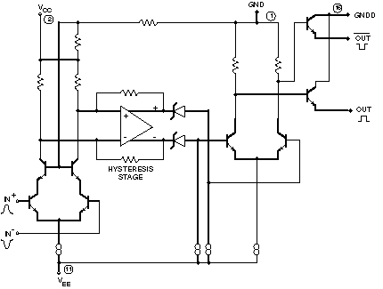
The MVL107S incorporates a unique hysteresis feature for exceptionally clean operation. When the comparator changes state, an internal differential input offset of nominally 4.8 mV is generated. This positive feedback drives the device quickly through its switching region, greatly reducing the possibility of oscillation or output chatter with small or slowly changing inputs. The propagation delay is typically 3.5 nsec and changes by only 100 psec across a 5 to 100 mV overdrive range. This very low delay variation makes this comparator extremely useful in critical timing applications.
The MVL107S provides differential inputs and complementary outputs compatible with the ECL logic family. The outputs can drive 50 ohm loads or 100 ohm twisted pair. (External pull-down resistors are required.)
| MAXIMUM RATING | ||||||
| Symbol | Parameter | Min |
Typ |
Max |
Units |
Comments |
| Vcc | Positive Supply Voltage | 5 | 6 | V | ||
| VEE | Negative Supply Voltage | -5.2 | -6 | V | ||
| Input Voltage | �4.0 | V | ||||
| Differential Input Voltage | �3.6 | V | ||||
| Output Current | 30 | mA | Per output pin | |||
| Power Dissipation | 80 | mW | ||||
| T | Operating Temperature | 0 | 25 | 70 | � C | |
| ELECTRICAL CHARACTERISTICS | ||||||
| Symbol | Parameter | Min |
Typ |
Max |
Units |
Comments |
| IOS | Input offset current | -0.5 | �0.05 | 0.5 | �A | |
| IB | Input bias current | 1.6 | 3.5 | 6 | �A | |
| Rin | Input resistance | 20 | 30 | Kohm | ||
| Cin | Input capacitance | 1.2 | 1.6 | 2.1 | pF | |
| Vcm | Input voltage range | -2 | 1.7 | V | ||
| VT | Threshold | 0 | 2.6 | 6 | mV | |
| VH | Hysteresis voltage | 4.4 | 4.8 | 5.2 | mV | |
| VOL | Output low level | 1.95 | -1.8 | -1.6 | V | RT > 510 ohm, VT > -5.2 V |
| VOH | Output high level | -0.91 | -0.79 | -0.74 | V | RT = 510 ohm, VT = -5.2 V |
| I+ | Positive supply current | 5.5 | mA | |||
| I- | Negative supply current | 6 | mA | |||
| PD | Power dissipation | 59 | mW | |||
| SWITCHING CHARACTERISTICS | ||||||
| Symbol | Parameter | Min |
Typ |
Max |
Units |
Comments |
| tpd | Propagation delay | 3 | 3.5 | 4 | nsec | 50 mV overdrive Note 1 |
| delta tpd/delta T | Avg. Temp. Const. of prop. delay | 2 | psec/�C | 0 to 70�C | ||
| tr, tf | Transition time | 1 | 1.4 | 2 | nsec | RT = 510 ohm;VT = -5.2 V |
| DPR | Double pulse resolution | 3.8 | nsec | Note 2 | ||
| fmax | Max. toggle frequency | 350 | MHz | |||
| Tmin | Min. input width | 2 | nsec | |||
1. Propagation delays are defined as the delay between a positive going input and an output transition of either polarity. The input overdrive is 50 mV with the threshold set at 0 mV.
2. Double pulse resolution is defined as the minimum pulse pair spacing at which the MVL107S responds to the second pulse of the pair. The output levels of the second pulse must cross V OH and VOL.
3. Characteristics measured at VCC = +5.0 V, V EE = -5.2 V and T = 25�C.
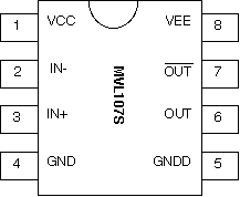
MVL107S Pin Assignments.so8 Package.
Copyright� February 1997. LeCroy is a registered trademark of LeCroy Corporation. All rights reserved. Information in this publication supersedes all earlier versions. Specifications and prices subject to change without notice.