Two identical power semiconductor devices are connected in a
half-bridge configuration. There are three testing modes for the lower
(LO) device and same three testing modes for the upper (HI) device.
Measuring the HI device requires an appropriately-rated HV isolated
probe, with the HV isolation equivalent to the DC Bus voltage.
- Test Mode 1: The tested device is in the ON state and conducting
current, the other device is OFF.
- Test Mode 2: The tested device is in the OFF state and blocking
current, the other device remains OFF.
- Test Mode 3: The tested device is again in the ON state and
conducting current, the other device remains OFF.
The inductor is set to switch position 1 and the circuit is
operated in three consecutive modes. First, the LO device is driven ON
by a simulated gate-drive pulse and the HI device operates in a
free-wheeling mode (left image). Then, the LO device is driven OFF
(middle image) and current continues to flow in the inductor (but does
not increase). Finally, the LO device is driven ON again and
reverse-recovery diode current briefly flows through the HI diode
shortly after the transition to ON condition, adding to the LO device
conduction current during this time (right image). During operation in
all three modes, the LO device gate-drive pulse and LO device output
voltage and conduction current is measured.
The inductor is changed to switch position 2 and the circuit
is operated in three consecutive modes. First, the HI device is driven
ON by a simulated gate-drive pulse and the HI device operates in a
free-wheeling mode (left image). Then, the HI device is driven OFF
(middle image) and current continues to flow in the inductor (but does
not increase). Finally, the HI device is driven ON again and
reverse-recovery diode current briefly flows through the LO diode
shortly after the transition to ON condition, adding to the HI device
conduction current during this time (right image). During operation in
all three modes, the HI device gate-drive pulse and HI device output
voltage and conduction current is measured.
Engineers designing and using power semiconductor devices
want to minimize losses during switching and conduction operations to
maximize efficiency. Engineers must:
- 1. Accurately measure gate-drive (Vgs) signal rise time and signal
fidelity/shape on both LO and HI devices (Vds)
- 2. Precisely measure device output voltage during switching,
conduction, and off (blocking)
- 3. Precisely measure drain current and calculate efficiency during
various operating modes
- 4. Accurately characterize the diode's reverse-recovery current to
calculate energy and efficiency losses (for MOSFETs)
Teledyne LeCroy is uniquely able to offer the highest
precision oscilloscopes and probes (and complimentary hardware and
software) for the most accurate and precise device characterization.
- 12-bit high definition oscilloscopes (HDO®) with 0.5% gain accuracy
and lowest noise at full bandwidth
- Optical and electrical isolated voltage probes with superior CMRR,
high accuracy and precision calibrations
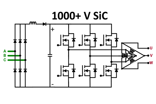
- Probes custom-tailored to the needs for 60 V GaN, 500 V GaN, and
1000+ V SiC testing
- Complementary power supplies, signal generators (AWG/AFG),
measurement software, and test automation software