Radar Signal Analysis With Oscilloscope Demodulation
Learn how oscilloscope demodulation and FFTs reveal radar pulse envelopes, Barker-coded phase modulation, chirp behavior, and frequency content.
Learn how oscilloscope demodulation and FFTs reveal radar pulse envelopes, Barker-coded phase modulation, chirp behavior, and frequency content.

This article explains the expected behavior of on-die power rails during CMOS switching events, including PDN current flow, clock-edge noise, and asymmetric current draw between switching and latching operations.

Learn how oscilloscope histograms help characterize component specifications by comparing propagation delay, mean, standard deviation, and measurement spread under different conditions.

Accurate on-die power rail measurements depend on proper sense-line design, differential probing, and careful test setup at the package level.

Armed with a suitable oscilloscope and active voltage-rail probe, you're now ready to make some power-rail measurements on a semiconductor die. Of course, making measurements on a die is a little different than making measurements on a printed-circuit board. This is where careful design-for-test at the die level comes in, because the chip, its packaging, and the board on which it will be mounted must be instrumented so as to make the on-die measurements possible.
Let's describe the technique most commonly used in the industry to measure voltages on the die itself. To measure the power-rail voltages on the die, you obviously need to be able to probe the rail. The connections coming off the die are routed to the bottom of the die to ball-grid-array (BGA) balls. Taking measurements directly from the die itself is a difficult task, so it's common to take the measurements from packaged devices.
If the die and package designers have done their jobs correctly, then the die will be packaged in such a way as to have sense lines from any Vdd or Vss core pads on the power rail all the way through the package (Figure 1). These direct path sense lines must not be connected to the package's power-delivery network (PDN) or to the board's PDN, but come unhindered to BGA balls on the bottom of the package.
Generally speaking, it is with these sense lines that we will measure both the Vss and the Vdd on the die. We'll measure these voltages with two probes in differential fashion. The potential between Vss and Vdd is the voltage on the die that we're interested in.
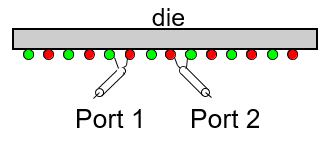
Now, if you do not have a package instrumented in this fashion, you can't really look at the on-die measurements directly (in a subsequent post, we'll describe an indirect method). But if you do have a properly designed die and package, not only can you measure the on-die voltages, but you can also measure on-die impedances and the impedances of the PDN. Note that the latter requires two-port access to the die as shown in Figure 2.
As an aside, if you do have your chip package instrumented in this way, you can still use that package for production devices. You might have had a test (or bring-up) board instrumented with the separate, isolated power rails so as to more easily make the on-die measurements. Then, on the production PCBs, you'd connect these sense-line balls to the board's PDN. So it's not sharing the power rail on the package, but in all likelihood a lot of I/O connections will do so. This is why you can use the same instrumented package for both bring-up testing and for production.
With a properly designed die, package, and board, you can take three Vdd current waveform and response measurements that will tell you all you need to know about the PDN: the single clock-impulse response, the step response for PDN current transients, and a resonance response. Taking these measurements requires that you have a sense-line connection straight to the core of the die. But even if you don't, there's another way to skin this cat, and we'll describe it in another post.
Copyright © 2020-2026 Teledyne LeCroy. All rights reserved. All original content, including text and photos, is the property of Teledyne LeCroy and cannot be reproduced without expressed written permission.

This article explains the expected behavior of on-die power rails during CMOS switching events, including PDN current flow, clock-edge noise, and asymmetric current draw between switching and latching operations.

Instrumented microcontroller boards and active voltage-rail probes make it possible to directly observe on-die power rail behavior, including sag, noise, and ground bounce.

Dr. Eric Bogatin answers common ground bounce questions covering dI/dt, quiet-low measurements, return path discontinuities, via placement, TDR, and differential probing.

This article introduces the RP2060 and RP4060 power rail probes, designed for modern 48 V power architectures with high offset capability, low-noise measurements, and high-bandwidth power integrity analysis.
