Radar Signal Analysis With Oscilloscope Demodulation
Learn how oscilloscope demodulation and FFTs reveal radar pulse envelopes, Barker-coded phase modulation, chirp behavior, and frequency content.
Learn how oscilloscope demodulation and FFTs reveal radar pulse envelopes, Barker-coded phase modulation, chirp behavior, and frequency content.

This article explains the expected behavior of on-die power rails during CMOS switching events, including PDN current flow, clock-edge noise, and asymmetric current draw between switching and latching operations.

Learn how oscilloscope histograms help characterize component specifications by comparing propagation delay, mean, standard deviation, and measurement spread under different conditions.

This article explains the expected behavior of on-die power rails during CMOS switching events, including PDN current flow, clock-edge noise, and asymmetric current draw between switching and latching operations.

Now that we're ready to begin some on-die power-rail measurements, it's a good idea to step back for a moment and anticipate what these measurements should show us. What actually happens on the die when CMOS gates are switching on and off? What should we expect to see on the on-die power rails? And what happens at the clock edges?
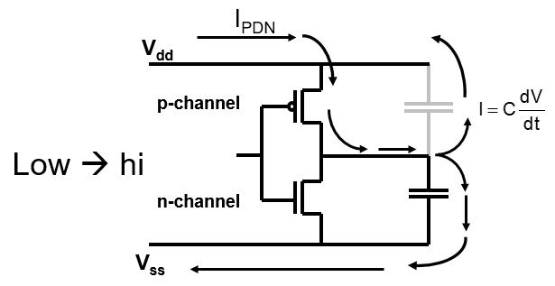
When the P-channel device (or any gate on the die, for that matter) switches from logic low to logic high, noise from the power-distribution network (PDN) on the die will flow from the Vdd/Vcc rail all the way through to the Vss rail (Figure 1). This is because the capacitance of the output line is referenced to the capacitances of both rails when the device switches from low to high.
What happens when the device switches from high to low (Figure 2)? It's logical to think that it would simply discharge the capacitance across the N-channel gate and that current flow would be local to that loop. But on the die (and sometimes also on the board), that output capacitance is also referenced to Vdd/Vcc through the P-channel capacitance. Thus, when the output line switches from logic high to logic low, yes, we discharge the current in that capacitor across the N-channel gate. But we also have a voltage drop through the P-channel capacitor, and the dV/dT means that current is flowing there, too.
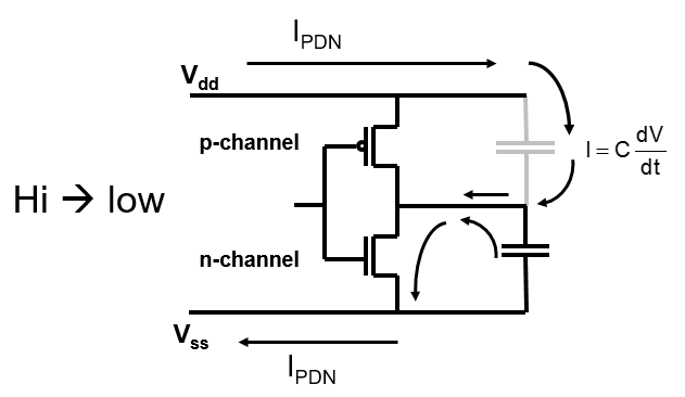
So even when we go from logic high to logic low, we will still have PDN current flowing through the PDN's impedance. That, in turn, means that we will see current flowing on both edges of the clock.
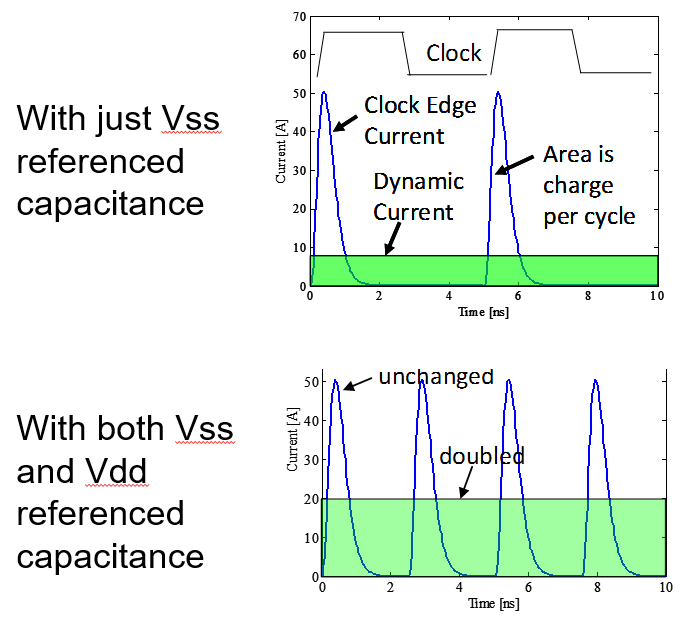
In looking at both edges of the clock, we expect to find that when the clock turns on, all the gates are typically edge-switched. Generally speaking, depending on the logic design, when the clock edge rises, the gates are switched, and when the clock edge falls, the gates are latched. In latching, there should be less current draw than in switching. So even though we get PDN current flowing between Vdd/Vcc and Vss on both clock edges, there should be an asymmetry in that current flow (Figure 3).
That sums up our expectations of what we should see on the on-die power rails. Next time, we'll look at the actual measurement results.
Copyright © 2020-2026 Teledyne LeCroy. All rights reserved. All original content, including text and photos, is the property of Teledyne LeCroy and cannot be reproduced without expressed written permission.

Instrumented microcontroller boards and active voltage-rail probes make it possible to directly observe on-die power rail behavior, including sag, noise, and ground bounce.

Dr. Eric Bogatin answers common ground bounce questions covering dI/dt, quiet-low measurements, return path discontinuities, via placement, TDR, and differential probing.

This article introduces the RP2060 and RP4060 power rail probes, designed for modern 48 V power architectures with high offset capability, low-noise measurements, and high-bandwidth power integrity analysis.


Accurate on-die power rail measurements depend on proper sense-line design, differential probing, and careful test setup at the package level.